General Description:
The Advanced Packaging Solutions (APS) Group is part of the RF and EO/IR Subsystems Department, which is a highly talented team of scientists and engineers with diverse backgrounds in electromagnetics, Radio-Frequency (RF), analog, digital, and microelectronics packaging & assembly. The mission of the group is to develop state of the art active and passive components, modules, and packaging solutions for next generation RF & Millimeter-Wave (mmW) subsystems such as Radar, Communications, and Electronic Warfare. We seek a self-motivated scientist / engineer with strong communication and leadership skills to serve as the lead for the APS Group. The role consists of approximately 25% management and 75% technical contributions.
Essential Duties:
Line management duties include managing resources, talent acquisition (e.g., recruiting), staff professional development/mentorship and additional department-wide, lab-wide, and HRL-wide strategies & assignments.
Technical duties require candidate to participate in the development of lab-wide strategies, lead research and development of novel 2.5D and 3D heterogeneous integration technologies for RF and mmW applications (e.g. next generation RF/mmW Phased-Array Systems), with attention to all facets of this endeavor from conceptual design phase considering electrical, thermal, mechanical design constraint to engineering and manufacturing, as well as verification and validation phase.
Provide mentorship and guidance to others in all aspects of these projects (technical, organization, reporting, etc.).
Organize and present results, in written reports, journal papers, and oral presentations.
Create and manage work plans to meet or exceed schedule deadlines and technical expectations.
Strong leadership and contributions to proposal and marketing efforts required to sustain continued R&D efforts.
Required Skills:
More than 15+ years of hands-on experience with developing novel 2.5D and 3D microelectronic packaging and heterogeneous integration for RF & mmW microsystems.
At least 3-5 years of experience in a role involving leadership of highly trained technical staff
Extensive experience with design of experiments and analysis techniques (electrical, mechanical, thermal, chemical, etc.) needed to develop and assess new process integration modules and techniques.
Experience with leading US government proposal and marketing activities. Demonstrated experience developing external partnerships and vendor relationships.
Several years of experience in organizing and leading technical research and development efforts, and in preparing presentations and proposals needed to attract research funding.
Experience with traditional as well as advanced packaging techniques (e.g. ceramic and laminate chip-level packages, printed circuit boards, SoC, SiP, MCM, HD interposers, etc.).
Hands-on experience with semiconductor microfabrication is a plus.
Candidates should possess a proven track record of developing novel and successful solutions to complex technical issues.
Extensive knowledge of RF/mmW (0.1-200+ GHz) with strong electromagnetic (EM) background.
Extensive knowledge of semiconductor microfabrication
Knowledge of multi-physics simulation tools (e.g. ANSYS, COMSOL), high frequency and RF simulation tools (e.g. ADS, MWO, Cadence), electromagnetic simulation tools (e.g. HFSS or CST)
Familiarity with digital, mixed-signal, power and signal integrity
Knowledge of system engineering, program and project management is a plus.
Understanding of material science, surface chemistry, semiconductor physics, and thermal/mechanical theory related to electronics processing and assembly techniques is a plus.
Proficiency in use of computers, engineering workstations, and complex electronic equipment
Proficient in oral and written communication
Ability to interact with vendors/colleagues and willingness to work in a fast-paced, deadline-driven environment.
Ability to work well in a team and independently.
Required Education:
MS or Ph.D. degree in Electrical Engineering, Mechanical Engineering, Physics, or related scientific discipline.
Physical Requirements:
Must be sufficiently mobile to work within confined spaces and have both visual and hearing acuity.
Special Requirements:
US citizen status is required. Active security clearance is a plus.
Compensation:
The base salary range for this full-time position is $182,720 - $234,168 + bonus + benefits.
Our salary ranges are determined by role, level, and location. The range displayed on each job posting reflects the minimum and maximum target for new hire salaries for the position. Within the range, individual pay is determined by work location and additional factors, including job-related skills, experience, and relevant education or training. Your recruiter can share more about the specific salary range during the hiring process. Please note that the compensation details listed reflect the base salary only, and do not include potential bonus or benefits.
Top Skills
What the Team is Saying


What We Do
HRL Laboratories, LLC, Malibu, California, (hrl.com) pioneers the next frontiers of physical and information science. Delivering transformative technologies in automotive, aerospace and defense, HRL advances the critical missions of its customers. As a private company owned jointly by Boeing and GM, HRL is a source of innovations that advance the state of the art in profound and far-reaching ways.
Why Work With Us
Our success is the result of our collaborative team of researchers, many of whom are the leading experts in their fields. Through their insights in support for our customers, we are finding the unique opportunities in technology.
Gallery
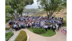


HRL Laboratories Offices
Hybrid Workspace
Employees engage in a combination of remote and on-site work.
Hybrid Policy is role specific.